This post intends to help understand what is SMT, why is it used and explain each SMT process and their most common business requirements.
Topics
- What is SMT?
- What does it process?
- SMT Line
- SMT Processes and Common Requirements
What is SMT?
Well, SMT stands for “Surface Mount Technology” and it’s a method used in the electronics industry to manufacture electronic circuits onto printed circuit boards (PCBs). It involves mounting electronic components, such as resistors, capacitors, integrated circuits, and so forth, directly onto the surface of the bare board.
Back in the 1960s, IBM came up with what they called “Planar Mounting,” which later evolved into Surface Mount Technology (SMT). They used this new method to build smaller computers, ditching the old-school Through-Hole Technology (THT). In the THT era, components were stuck onto circuit boards by inserting their leads through drilled holes and then they’d solder them in place.
 \
\
Through-Hole Technology
 \
\
Surface Mount Technology
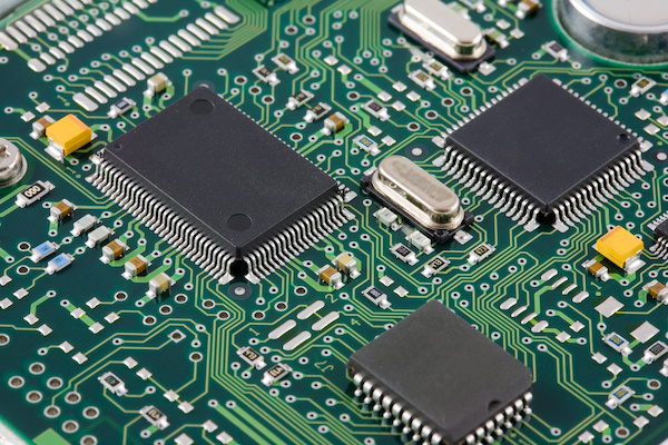
Everyone knows how an electronic board looks like, a green piece full of components, some big ones and others really really small ones, almost not visible through naked eye. I will explain the process of how the components actually get to the board.
 \
\
Electronic Circuit Board
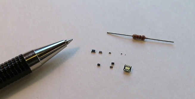
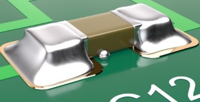
Electronic components size comparison
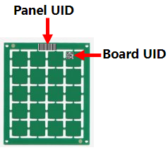
WIP - Panels, Boards and Reference Designators
Before moving to the SMT processes it’s important to understand the basic concepts of the materials that will be in process in the SMT Line, the PCBs.
A PCB can just have a single board or it can be a multi board panel. Although this convention might not be used by everyone, normally what we call panel is the id of the frame of the PCB and what we call board or arrays are the ids of the units inside the panel.
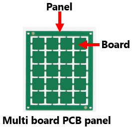
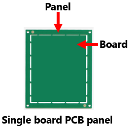
Panel with multiple boards inside (left) and panel with just 1 board (right)
Tipically, there is a Production Order which is defined in quantity of boards. Then the structure of materials starts with a topmost material which is the Lot or WorkOrder that will have Panels as sub-materials and each Panel will have its own Boards. The Lot will be assigned to be processed in a line and each panel will be read in each equipment of that line.
Another important concept about the PCBs are the reference designators, these are the names of the positions inside a PCB where the components will be inserted. This is important because customer requirements regarding traceability, defects or data collection go to the reference designator level inside the board of the panel.
Below we can see an example (red arrows):
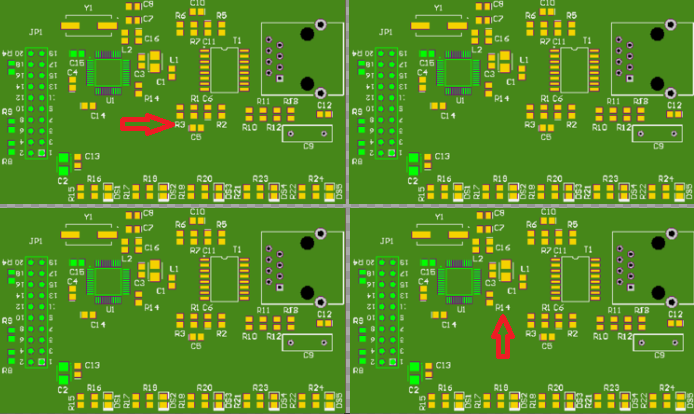
Panel with 4 Boards with identification of the reference designators
SMT Line
Let’s start the process walkthrough introducing the concept of Surface Mount Assembly Lines (SMT Line) and the first question is..
Why are SMT Lines used?
The main reasons to use SMT Lines are the fact that they are faster and more efficient than traditional assembly methods, they allow for a higher degree of automation, they reduce PCB assembly costs and the ease of PCB assembly using both sides of the board without the hole limitations.
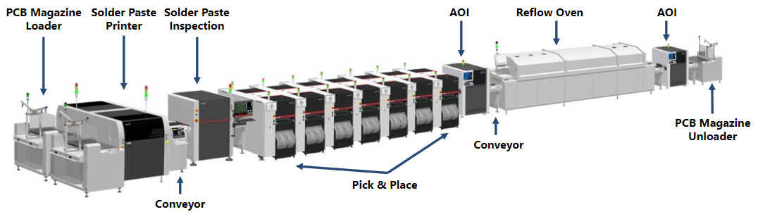
SMT Line
An SMT Line is composed by a group of machines process specific connected by conveyors:
- Solder Paste Printing - Printer
- Solder Paste Inspection - SPI
- Components Placement - Pick&Place
- Reflow Oven - Reflow
- Automatic Optical Inspection - AOI
This is the normal sequence of processes that can be seen in SMT Lines, but there can be variations, for instance, there are lines that have an AOI before the reflow oven and another AOI post reflow or lines that have the AOI process out of the line. All this configurations will depend on the customer requirements for their products, the complexity of the products and the maximum optimization of equipment efficiency and quality.
There are different types of PCBs but the most common scenario is to have 2 sides to be populated. The line just needs to be configured for each side (commonly called Bottom and Top sides), with the right recipes/programs, list of components to assemble (BOMs) and tools to be used (durables).
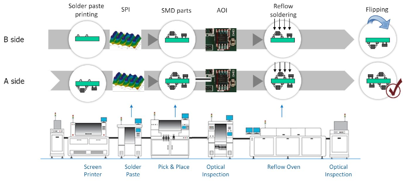
SMT Process - Double Side
There are also PCBs populated only in one of the sides.
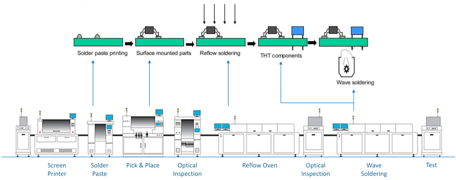
SMT Process - Single Side
Whether the PCB has 2 sides or just 1 side to be populated it can have a THT process after the SMT process.
Now, let’s see 1 by 1 each of the SMT processes and the most common use cases.
Laser Marking (Laser - LMK)
Crucial to ensure full traceability over the entire process chain, PCB serialization is one of the first steps in PCBA. Each panel and/or board(s) receives a unique ID that will be used for singular traceability over the entire product flow.
Nowadays, serialization is becoming far more common by using a laser mark machine that engraves each panel and/or board with its unique ID, however, there’s still other methods such as label printers and manual operations.
Panel and Boards Serialization
What are the typical MES requirements
The main requirement for the serialization process is define who is the owner of the IDs generation for panels and boards and make sure that we know exactly the relation between them. It’s important to maintain full traceability over each manufacturing process per individual material id.
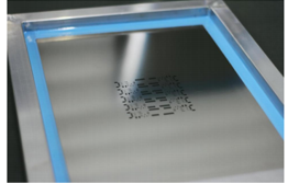
Solder Paste Printing (Printer - SPP)
After loading the PCBs to the line, through a loader of magazines or a destacker, the 1st process of the line is the solder paste printing where the machine deposits the correct solder paste volume onto each of the PCB pads that will be populated with components to be soldered. This is done by forcing each bare PCB through a stencil (solder mask) that is product specific and spreading the solder paste onto the surface of the stencil with squeegees. Below, there’s a diagram explaining the process and the tools that are used.
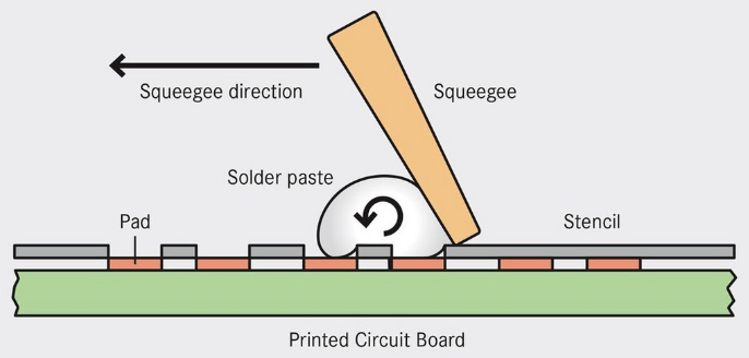
Solder paste printing process
 \
\
Stencil and Squeegee
What are the typical MES requirements
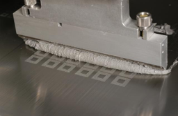
The solder paste composition and deposition are critical factors influencing the quality and reliability of the final product. One of the key aspects regarding the printing process is the Solder Paste Management which involves track the solder paste tubes from the moment they arrive to the shopfloor, storage and usage condition.
The most common tools that requires to be tracked in the printer machine are the stencil and squeegees. Stencils ensure accurate transfer of solder paste onto the board, defining the shape and volume of each deposit. Squeegees are tools used to spread the paste evenly across the stencil’s surface. The angle, pressure, and speed at which the squeegee traverses the stencil influence the thickness and consistency of the deposited solder paste.
The quality of this process can only be assured if the stencil and squeegees usage, in terms of number of prints or time at the machine, are controlled so, a typical requirement of the customers is to have the stencil and squeegee management.
Solder Paste Inspection (SPI)
To verify the quality and accuracy of the paste printing process, automatic solder paste inspection machines are used to inspect and detect if each PCB pad received the correct amount of solder paste.
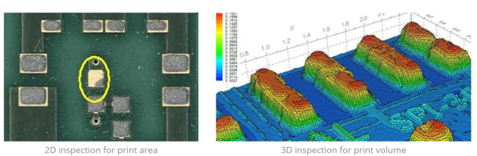
Solder paste inspection
If the machine detects a defect in a pad, which could be from excessive or insufficient solder paste, a bridge between pads or a deviation from the correct position for example, it will mark the defect in that PCB in a specific reference designator and an operator needs to review it.
This operator validation requires the operator to check the defect and decide if it’s a real defect, which could mean a PCB sent to a wash station or scrap the board for example, or if it’s a pseudo defect and the PCB is good to go in the process. Off course this is the common scenario but, there can always be specific behaviors, depending on the customer, to handle each type of defect.
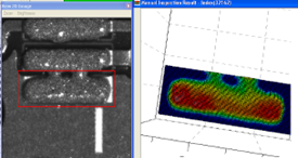
Defect: Bridge
Defect: Offset
What are the typical MES requirements
The key requirements in this process are the program validation, which means ensure that the PCB is being inspected with the appropriate program and capture the defects at the board and reference designator level as well.
Placement (Pick & Place - P&P)
The general concept of the component’s placement process is where SMD components will be assembled by the machine in the right position (reference designator) of each PCB.
Each component is picked from its packaging (reel or tray) using either a vacuum or gripper nozzle, checked by the pick and place machine vision system and placed in the programed PCB location at high speed, accordingly with the machine’s recipe and setup.
Pick and Place machines can be single or dual lane and they can have 1 or more locations. Below there’s a figure explaining the concept of lanes and locations.
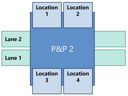
Example of a Pick & Place machine layout
Locations in a placement machine represent the place where a Change Over Table (or Feeder Table) can be docked and more locations means machines with higher capacity.
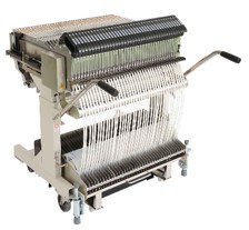
SMT Change Over Table (Feeder Table)
SMD components in forms of reels need to fed into the PCBs and the tool that is responsible for this process are the SMT feeders. The feeders are prepared with the reels attached and mounted onto a feeder table. Bigger components can also be fed in trays and they are directly supplied to pick and place machines with tray modules.
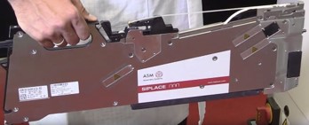
SMT Feeder
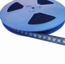
SMT Reel
What are the typical MES requirements
The placement of electronic components in the PCB is likely the most complex process in the SMT line and because of that the key indicator of an SMT area (known as CPP - Cost Per Placement, but let’s leave this SMT KPI discussion for a future post). Since this is the most important process of the line these are the most common requirements from customers:
- Bill-Of-Materials Management: Control component quantities, reference designators, and placement locations. It should ensure that the correct components are picked and placed according to the BOM for each assembly. This envolves to validate the BOM/Setup before production starts and every time a PCB is produced in the line check the consumptions against the BOM.
- Material Handling: Manage the movement and tracking of components throughout the pick-and-place process and support material traceability, lot tracking, and FIFO (First-In-First-Out) inventory management to prevent material mix-ups and ensure product quality.
- Material Traceability: Record full traceability from the reel condition until the specific reference designator. The reference designator R123 from board 1 in the panel A consumed a component from the reel ABC at the feeder X in the Feeder Table Y and Pick & Place 3.
- Recipe Management: Before production starts and also while production is running, validate that the program in use at the machine match the respective program of that product.
Solder Reflow (SOL)
It’s the most widely used method to weld SMDs to PCBs. In this process, PCBs passes through a reflow oven machine where all the electrical solder connections between components and PCB will be formed by heating the PCB to a sufficient temperature to melt the solder paste.
This may appear to be one of the less complicated parts of the SMT processes, however, each product has a specific temperature profile considering the components that are part of it, so it’s important to validate and keep track of the machine’s recipe to ensure quality solder joints, without damaging the components or PCBs due to excessive heat.
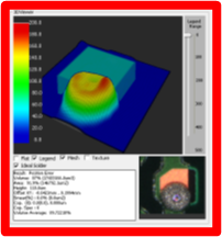
Reflow process
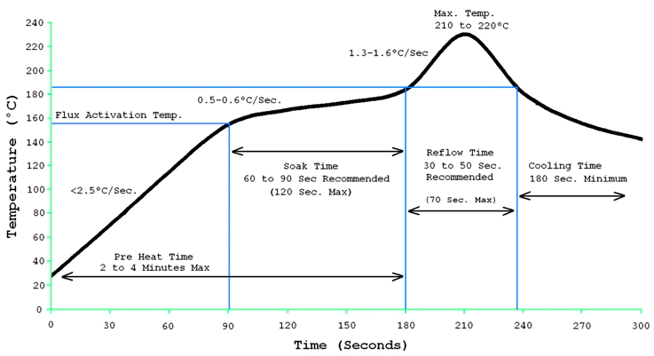
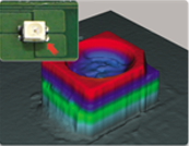
Reflow profile example
What are the typical MES requirements
The program validation is key to this process, to make sure that the temperature profile match to the PCB product otherwise it could result in scrap. There can also be requests to capture the oven parameters for each PCB for traceability purposes.
Automatic Optical Inspection (AOI)
Process to inspect the quality and accuracy of the SMT assembly process. Can be used at many steps of the manufacturing process including bare PCBs, pre and/or post-reflow soldering.
Using high resolution cameras, AOI machines scan each PCB identifying possible defects that may lead to PCB failures. Supported by image processing software, images of the PCB and components where a possible defect occurred, are provided to an operator by the machine SW to be then evaluated.
Similar to the SPI, depending on the classification of the operator it could result on real defects and based on the type of defect, product, type of component or even reference designator the PCB can be scrapped, sent to rework, trigger a protocol for instance. It can be also classified as a pseudo defect and that means the PCB is good to go in the process.
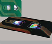
AOI - Missing Component and Polarity error examples
What are the typical MES requirements
The key requirements in this process are the program validation, which means ensure that the PCB is being inspected with the appropriate program and capture the defects at the board and reference designator level as well.
Depaneling
When the SMT process is over, the boards need to be detached from the panel/frame and this can be done with several methods such as Manual Breaking, Milling, Laser or Router.
Normally, the boards are connected to the PCB panel by narrow tabs that will be broken to separate the board(s) from the panel. This process occurs after all the components are placed and tested on the boards.
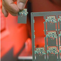
Boards being removed from Panel
What are the typical MES requirements
Know from which panel the board came from and ensure that the operator has visibility on which boards are good and which ones need to be scrapped.
The End
That’s it, we reached the end! It was a quick introduction on how SMT started and the main concepts related with it and its processes. We have also covered the most common requirements for each process and I really hope this information will be useful for you.
I would like to thank Hugo Leite, our Electronics Product Manager, for the information provided and valuable inputs to create this post.
Any question or if you want to discuss a bit more please feel free to contact me.
Author
Hello, my name is Fábio Reis ✌️
I’ve been working for 2 years at Critical Manufacturing and in my previous professional experience I’ve worked directly with SMT processes for 6 years.
You can check me at LinkedIn
